
From silicon to silicon carbide: FBK develops innovative materials for next-generation electronics
November 18, 2026
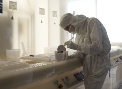
A scientific paper authored by four researchers from the Center for Sensors and Devices and published in Surfaces and Interfaces opens up new prospects for the production of SiC through a process developed entirely in FBK's clean rooms.
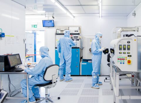
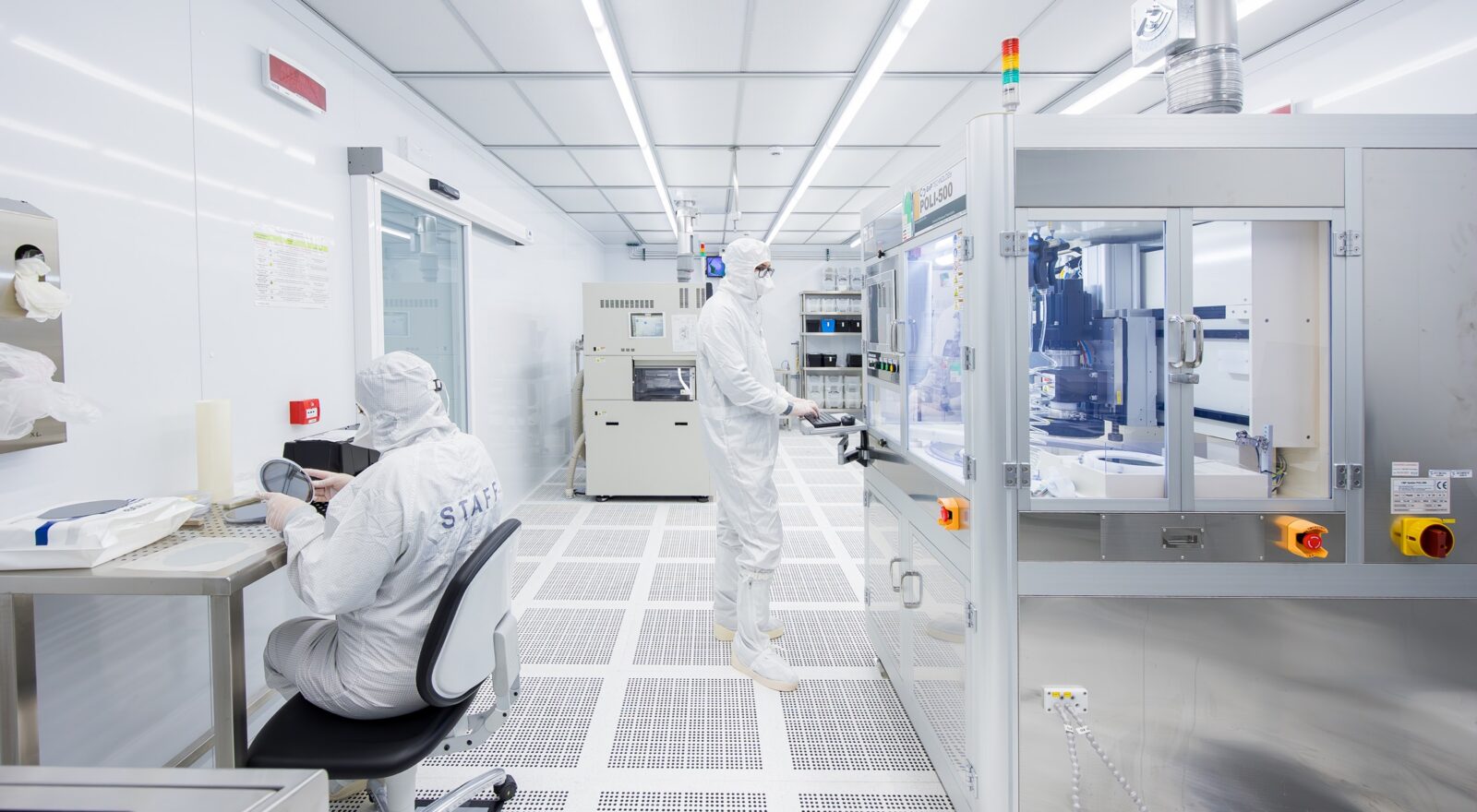
Fondazione Bruno Kessler is taking a new step in research on semiconductor materials used in electronics with the publication of its first scientific paper dedicated to silicon carbide (SiC). The paper, titled ““XPS analysis of substitutional carbon formation in silicon by recoil implantation from a PMMA film: A pathway to SiC synthesis” originated in FBK’s clean rooms and was published in the prestigious international scientific journal Surfaces and Interfaces, which has a high impact factor. The publication represents a first major milestone in FBK’s research into silicon carbide and demonstrates the value of collaboration across complementary scientific and technological expertise, exploring an innovative approach to incorporating carbon atoms into the silicon crystal lattice through a recoil implantation process from a PMMA (polymethyl methacrylate) film.
The authors are Giorgio Speranza, Andrea Pedrielli, Elia Scattolo, and Antonino Picciotto. “One of the most interesting aspects of the proposed technique,” points out Antonino Picciotto, author of the article and head of the NEXT research unit at FBK’s Center for Sensors and Devices, “is its compatibility with standard photolithography processes and with focused ion beam (FIB) technology. This feature could enable localized carbon implantation, leveraging technologies that are already well established in the microfabrication industry. The potential applications span strategic areas such as power electronics, radiation and particle detectors, and energy storage systems—sectors in which silicon carbide, thanks to its wide-bandgap semiconductor properties, offers significant opportunities for the development of increasingly efficient and high-performance devices.”
The result is the outcome of multidisciplinary collaboration among various research units at FBK’s Center for Sensors and Devices, specifically NEXT (New opportunitiEs eXploitation process and Techniques for Sensors and Devices Applications), MTSD (Materials and Topologies for Sensors and Devices), and IQ&O (Integrated and Quantum Optics). The NEXT research unit was recently established with the aim of exploring new technological opportunities and developing innovative processes and techniques for applications in sensors and devices. “The publication of this article,” says Giorgio Speranza, author and senior researcher in the MTSD research unit at the same center, “therefore represents the achievement of an important goal that demonstrates, on the one hand, the ability of FBK’s research groups to conduct state-of-the-art basic research and, on the other, their ability to translate insights into concrete results with high technological potential.”
The result is part of a broader program of technological and infrastructural growth at the Foundation, also supported by strategic initiatives such as IPCEI Microelectronics and Communication Technologies (IPCEI ME/CT) and projects dedicated to Wide Band Gap Chips JU (WBG) technologies. These significant investments are contributing to the construction of a new building and state-of-the-art laboratories designed to house and develop emerging technologies in the field of semiconductors, including silicon carbide. This strategic path links today’s research results to tomorrow’s new infrastructure, skills, and opportunities for industrial innovation, strengthening FBK’s role in the development of enabling technologies for the microelectronics of the future.
The author/s
Related articles